Jul 31, 2019

ZENER DIODE


ZENER DIODE:
 Zener diode is used as a voltage regulator. It provides stable reference at the output and operated always in reversed bias direction. The PN junction is heavily doped to construct the Zener diode, when we diode operated in reversed bias the early breakdown is called Zener breakdown, it’s a normal breakdown  all the application is operated in this breakdown after applying higher voltage then the breakdown changed in avalanche breakdown now in this breakdown the diode then not able to use again. The breakdown as
zener diode model
Zener diode
 AVALANCHE BREAKDOWN:
 In this breakdown the voltage is greater than the Zener voltage and hence it damaged and flow maximum voltage. Once time a diode is operated in avalanche breakdown than it can’t use another time it became useless.
ZENER BREAKDOWN:
Diode can be used again if it operated one time in Zener breakdown, in this breakdown the voltage is less than the avalanche breakdown the application is run in Zener test current region. If we considered that the Zener breakdown is operated in 5V than the avalanche is must greater then 5V. 
ZENER IMPENDENCE:
 The total resistance in a circuit is called impendence
From ohm,
                V=IR
And 
                 R=V/I
Where
                 R=Zz, V=Vz, I=Iz
Hence Zener impendence 
                 Zz=∆Vz/∆Iz  
NUMERIC 1:
A Zener diode exhibit a certain changed in Vz for a certain Changed in Iz on a portion of the linear characteristic curve between Izk and IzM in fig. what is the Zener impendence 

Solution:
              ∆Vz= 50mV
              ∆Iz= 5mA
               Zz=?
Here Zener impendence (Zz)=  ∆Vz/∆Iz 
              Zz= 50mV/5mA
                   = 10Ω
   

POWER SUPPLY FILTRATION(Capacitor as a filter)


POWER SUPPLY FILTRATION:
  When we convert AC into DC we had a problem that the signal has two states as shown fig (a) but we need straight line DC signal as shown in Fig (b).

Here we need something material that changed the eliminate the states and changed into a straight line as in fig (b) for this reason we use power supply filter which will be a capacitor.

CAPACITOR AS A FILTER:
   We used a capacitor with suitable farad (farad is unit of capacitor) as the capacitance of capacitor is high make a perfect DC where capacitance is the capability of storing charges or current.
Capacitor as a filter,power supply filtration
Capacitor as a filter

After placing capacitor the output signal will like as shown in fig.

Where the value of r, V(rect), Vdc, Vrp.p is given below


Numeric 1:

  Determine the ripple factor for the filtered bridge rectifier with the load indicated in fig.

Data:
        Vin = 120Vrms
         Frequency =120Hz
        Number of turn =ᶯ = 10/1 = 0.1
        Capacitance = C= 100µf
        Limiting resistance = RL =220Ω
       Ripple factor = r =?


BRIDGE RECTIFIER


BRIDGE RECTIFIER:
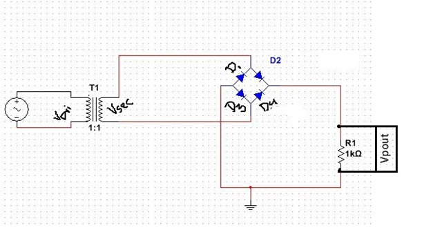
 In replacement of full wave rectifier we use Full wave bridge rectifier for rectification, change AC to DC current. But the question is here why we replace full wave rectifier, because bridge rectifier is more reliable than full wave it provide quantity of DC current as output. Overall the phenomenon of working of bridge is likely as full wave.

CONSTRUCTION:
bridge rectifier,full wave bridge rectifier
Bridge rectifier

DERIVATION:
          (1)     Vavg =Area/time =  2Vp /ã„«

          (2)     Vpout = Vpsec – 1.4 where
            Vpsec = Number of turn * primary volt = Õ² *Vpri
               If the primary voltage is given in rms then to find Vpri, multiply the rms value to 
              under root 2. same process goes for Vpsec
               Such as   Vpri = √2 *Vrms  
           (3)    PIV= Vpout + 0.7
NUMERIC =1

  Determine the peak output voltage for the bridge rectifier. Assuming the practical model. What PIV rating is required for the diodes? The transformer is specified to have a 12rms secondary voltage for the standard 120V across the primary.
Data:
                Vrms = 12V
                Vpout =?
Solution:
                Vpout = Vpsec – 1.4 where
                Vpsec =√2*12V 
                           = 16.97V
So
                 Vpout =16.97 -1.4
                            = 15.57V
And PIV required is
                  PIV = Vpout+ 0.7
                         = 15.57 + 0.7
                         = 16.2V

PEAK VOLTAGE:
                  P=V/I
            and I =P/V

HALF WAVE RECTIFIER


HALF WAVE RECTIFIER:
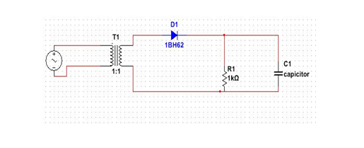
  Half wave rectifier is used to convert AC to DC. In half wave rectifier we use only on diode for rectification.Which gives high amount of ripple factor and only conduct either negative voltage or positive. it operate only one direction current due to use of only one diode.

CONSTRUCTION:
Half wave rectifier,What is half wave rectifier
Half wave rectifier

The signal of input and output shown in fig.

Half wave rectifier,What is half wave rectifier
Half wave rectifier

DERIVATION:

  First of all when we convert the AC to DC there should be a Vdc or Vavg to find Vavg we have
Half wave rectifier,What is half wave rectifier,numeric of Half wave rectifier
Half wave rectifier
                         

                                       (2)    Vp (out) = Vavg - 0.7

And 
                                       (3)     Peak inverse voltage = VIP
`                                                   VIP = Vp (in)


Numeric 1:
   What is the average value of half wave rectifier voltage?
Data:
            Peak voltage = Vp= 50V
            Pie = Ï€ =3.14
                  Vavg =Vdc =?
Solution:
                 Vavg= Vp/Ï€
                 Vavg = 50/3.14
                          = 15.92V


Jul 25, 2019

DIODE MODELS WHEN IT IS IN REVERSED BIAS:


DIODE MODELS WHEN IT IS IN REVERSED BIAS:
Same like forward biasing in reversed biasing we study about three models of diode.
      1.      Ideal model
      2.      Practical model
      3.      Complete model

IDEAL MODEL:
  In ideal model of diode in reversed bias we keep
diode model, diode, what is diode
diode model
 ‘ Ir’ is zero such as
Ir = 0
So by applying K.V.L rule we got the equation which is
Vbias – Vrlimit – Vr=0
Here
Vrlimit = Ir. Rlimit
And Ir is zero so Vrlimit also become zero
Hence
Vbias – 0 – Vr= 0
Vr = Vbias

PRACTICAL MODEL:
  In practical model the ’Ir’ remains zero such as
Ir = 0
diode model, diode, what is diode
diode model
So by applying K.V.L rule we got the equation which is
Vbias – Vrlimit – Vr=0
Here
Vrlimit = Ir. Rlimit
And Ir is zero so Vrlimit also become zero
Hence
Vbias – 0 – Vr= 0
Vr = Vbias


diode models, diode,what is diode
diode model
COMPLETE MODEL:
  In complete we considered all the resistance in circuit so there will be a value for ‘Ir’ which will greater than zero so ‘Ir’ will be something
Ir 0
By applying K.V.L rule we got 
Vbias – Vrlimit – Vr =0
Here
 Vrlimit = Ir. Rlimit and Ir 0
So
Vr = Vbias – Vrlimit

Jul 21, 2019

MODEL OF DIODE WHEN THE DIODE IS FORWARD BIAS:


MODEL OF DIODE WHEN THE DIODE IS FORWARD BIAS:
  When the diode is forward bias there are three type of model can be studied.
          1.      Ideal model
          2.      Practical model
          3.      Complete model

IDEAL MODEL:
  In ideal model we assume the Vf means the drop voltage through the depletion considered as zero. So
            Vf = 0
By applying K.V.L rule we got                   
Diode, Diode model
Model Diode
                                    
 Vbias – Vrlimit – Vf= 0
 Vrlimit = Vbias -     Vf                                                                              
Here 
        Vrlimit = Ir * Rlimit                                                                     
So
      Ir * Rlimit = Vbias – Vf                                                                   
And also note that Vf = 0
    Hence
      Ir=Vbias / Rlimit

PRACTICAL MODEL:
  In practical mode we considered the drop voltage through deletion region so we have Vf Is 0.7V thus the equation will be,
  Vf = 0.7V
By applying K.V.L rule we got    
Diode, Diode model
Diode model
  Vbias – Vrlimit – Vf = 0
  Vrlimit = Vbias - Vf
Here 
  Vrlimit = Ir * Rlimit
Hence 
  Ir * Rlimit = Vbias – Vf
  Ir = Vbias – Vf/Rlimit

COMPLETE MODEL:

 In complete model we considered the total resistance in diode so we have Vf and r’d which is the resistance of depletion region.
So 
Diode, Diode model
Diode model
    Vf= 0.7 + r’d
By K.V.L rule we got
    Vbias – Vrlimit – Vf = 0    
    Vrlimit = Vbias – Vf
Here
    Vrlimit = Ir (Rlimit + r’d)
    Ir (Rlimit + r’d) = Vbias – Vf
    Ir = Vbias – Vf/ (Rlimit + r’d)


DIODE:


DIODE:
  Diode is an electronic pn-junction device which is used to rectification. It consists of two material p-type and n-type material the region between P and N material is called depletion region.


Diode, What is diode, note on diode
Diode
  Diode is formed by doping. Doping is the process to construct a diode. Symbolically diode is represented by 

.


 In diode the P-type is covered more place by holes and  small number of electron, while in N-type the most of place is covered by electron and less area have holes.

RECTIFICATION:
  Rectification is a process in which alternating current is converting into direct current.
BIASING OF DIODE:
  There are two method of biasing in diode.
                1.       Forward biasing
                2.       Revised biasing

FORWARD BIASING:
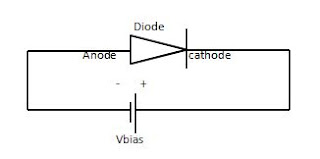
     In this type of biasing the diode acts as closed circuit because in this case the current is conduct through diode. To make the diode forward biasing connect the positive terminal of source to P type and the negative terminal of source to N type of diode as shown in figure  


  In this process the depletion region become narrow. And the voltage drop from the depletion region is 0.7V.  

REVERSED BIASING:
  In this type of biasing the diode acts as open circuit because in this case the current does not conduct through diode. To make the diode reversed biasing connect the negative terminal of source to P type and the positive terminal of source to N type of diode as shown in figure


In this process the depletion region becomes wider. And the voltage drop from the depletion region is zero because it acts as open switch but if we continuously supplying voltage then after 10 volt the depletion region blast and its going in break down region and the diode became useless, and maximum current flow through it .  

DIODE MODEL:
 There are three type diode models,
        1.       Ideal model
        2.       Practical model
  3.     Complete model

#  For complete detail of diode models in forward bias click here Continue
# And For complete detail of diode models in reversed bias click here continue